Ex-02a: GPIO Introduction
In this exercise you will learn the basic structure of a GPIO port. Next you will access the registers of a GPIO port. Like all memory-mapped devices, GPIOs are controlled by registers. For simplicity, a first configuration will be done using the debug interface. Finally, you will do your first implementation of a very simple application.
Objectives
Basic structure of the GPIO ports
Accessing registers with a debugger
Implement basic I/O functionality
Write and run a very simple application
Outcomes
Consult the GPIO peripheral datasheet.
Read and write registers to enable basic GPIO functions.
Get to know and use the CMSIS macros.
Learn how to read and write registers.
How to write and compile your own MCU program.
Description
Now that you have completed the basic programming courses, you should be familiar with basic concepts such as pointers. However, so far you have always used a pointer within a virtual address space. In the context of microcontrollers, particularly bare-metal operation without an operating system, you will need to work on the physical (real) memory addresses. Each address - in a memory mapped design - represents a register or part of a register. A register is an interface to a hardware function from a low-level software point of view.
Note
Only the Nucleo-64 board is used in this task.
Tasks
This section describes how to read the state of the buttons and how to change the state of a “GPIO” to switch an LED on or off.
Development Board Perspective (Nucleo-64)
On the development board you find a user push button (labelled B1) and a green LED (labelled LD2). Determine how the LED and button are connected to the microcontroller using the development board schematic, i.e. Nucleo-64 schematic. You will find the following information:
Question
How is each periphery element connected? (high or low active)
To which pin and port of the MCU is the element connected? (i.e. PF4)
Solution
Button (B1): The input is pulled up to VDD by resistor R30. When the button is pressed, the input is connected to GND and therefore reads a logic 0. The button is ACTIVE LOW.
LED: A logic level of 1 turns the LED on, therefore the LED is ACTIVE HIGH.
USER Button: PC13
LD2: PA5
Microcontroller Perspective (STM32 MCU)
You need to configure the appropriate pins to control the LED and button. Have a look at section 7 General-Purpose I/Os (GPIO) of the reference manual RM0390 reference manual. You must configure one pin as input and one as output. Take a closer look at 7.3.9 Input Configuration and 7.3.10 Output Configuration.
Question
Find the “region boundary addresses” of the ports you are about to use, i.e. “GPIOG 0x40021800”. This address is the base address from which the offsets are applied in order to access a specific register within the port.
Find the correct offset to access the “GPIO” registers within the port. i.e. “GPIOx_AFRH 0x24”.
Determine the active register(s) for the desired configuration. i.e. “GPIOx_OTYPER” has no influence when the “GPIO” is configured as an input.
Determine the reset value of the active register(s) for the current configuration, i.e. “GPIOx_MODER” of port A has a reset value unequal to zero. This may cause a conflict for some configurations.
Make a note of how you would configure the registers within the port to achieve the desired result.
How many registers does a STM32F446 “GPIO” port provide to control it?
List all registers and describe by one sentence its purpose.
Now that you have all the information you need to use the button, you need to test it. Should you start coding? Not yet, because there is an easier way to prove your assumptions.
Direct Manipulation
With a debug session running, you can observe and even manipulate (control) the register values. By using the debugger to prove your assumptions, you will be much faster compared to an implementation in e.g. C. If the assumptions are correct, a normal implementation using a programming language such as C is the next step. Use the debug interface to control the registers:
Exercise
- Enable the clock for the appropriate peripheral registers.
To do this, have a look at section 6 Reset and Clock Control (RCC) of the reference manual RM0390 reference manual and take a closer look at 6.3.10 RCC AHB1 peripheral clock enable register (RCC_AHB1ENR).
Configure the LED pin as an output and toggle the LED by changing the register values.
Are there several ways to switch the output of a “GPIO”?
If so, how do they differ?
Configure the user-button pin as an input and observe the input value while pressing the button.
Important
Remember that the debugger must be paused for register reads and writes.
Implementation
Now that you are confident with your configuration, you are ready for your first implementation.
Bit Manipulation
To read and write to a GPIO pin, it is usually necessary to change only one bit of a register and ignore the other, otherwise something unexpected will happen. To do this, we use the bit-wise operators that you have learnt in the previous courses. However, a few reminders follow to modify the desired bit in a byte.
Bit Manipulation
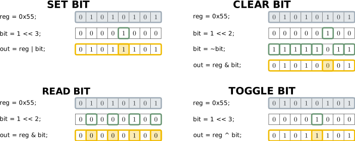
Example of bit manipulation using bit-wise operators in C
Main Function Structure
A first implementation will consist of two main parts. The first is initialisation, which ensures the correct configuration of the hardware. Every boot procedure goes through an initialisation phase of all its components. Second, the application, which implements a specific functionality. The application is usually implemented as a sequence of instructions that are looped forever.
Exercise
Before initialising your “GPIOs”, you must enable the clock on the specific port.
Inside the
main()function, just before thewhileloop [1], you have to add the initialisation for the “GPIOs”.Within the superloop, check for the button value and set the corresponding LED value.
Results
If all is well, your LED should show the current state of the USER button.
Exercise
Measure the current voltage levels of the GPIOs in use with the Saleae logic analyser.
Measure the reaction time of your MCU between a change of the USER button and the LED several times:
Is the response time always the same?
Is there a difference between turning the LED on and off?
Discussion
With your classmates, discuss the results of your measurements. If you have implemented different solutions, discuss whether a difference in the response time might be a consequence.